

本文介紹了LatticeECP3 FPGA系列主要特性,LatticeECP3-35簡化方框圖以及LatticeECP3視頻協議板主要特性,方框圖和詳細的電路圖。
Lattice 公司的LatticeECP3 FPGA系列能提供高性能的特性如增強的DSP架構,高速SERDES和高速源同步接口。LatticeECP3系列采用65nm技術,有149K邏輯單元和支持多達486個用戶I/O,可提供多達320個18x18乘法器以及各種并行I/O標準。廣泛用于批量生產的對成本和功耗敏感的有線和無線基礎設備以及各種多媒體設備。
LatticeECP3主要特性:
Higher Logic Density for Increased System Integration
• 17K to 149K LUTs
• 133 to 586 I/Os
Embedded SERDES
• 150 Mbps to 3.2 Gbps for Generic 8b10b, 10-bit SERDES, and 8-bit SERDES modes
• Data Rates 230 Mbps to 3.2 Gbps per channel for all other protocols
• Up to 16 channels per device: PCI Express, SONET/SDH, Ethernet (1GbE, SGMII, XAUI), CPRI, SMPTE 3G and Serial RapidIO
sysDSP™
• Fully cascadable slice architecture
• 12 to 160 slices for high performance multiply and accumulate
• Powerful 54-bit ALU operations
• Time Division Multiplexing MAC Sharing
• Rounding and truncation
• Each slice supports
–Half 36x36, two 18x18 or four 9x9 multipliers
–Advanced 18x36 MAC and 18x18 Multiply-Multiply-Accumulate (MMAC) operations
Flexible Memory Resources
• Up to 6.85Mbits sysMEM™ Embedded Block RAM (EBR)
• 36K to 303K bits distributed RAM
sysCLOCK Analog PLLs and DLLs
• Two DLLs and up to ten PLLs per device
Pre-Engineered Source Synchronous I/O
• DDR registers in I/O cells
• Dedicated read/write levelling functionality
• Dedicated gearing logic
• Source synchronous standards support
–ADC/DAC, 7:1 LVDS, XGMII
–High Speed ADC/DAC devices
• Dedicated DDR/DDR2/DDR3 memory with DQS support
• Optional Inter-Symbol Interference (ISI) ? correction on outputs
Programmable sysI/O™ Buffer Supports Wide Range of Interfaces
• On-chip termination
• Optional equalization filter on inputs
• LVTTL and LVCMOS 33/25/18/15/12
• SSTL 33/25/18/15 I, II
• HSTL15 I and HSTL18 I, II
• PCI and Differential HSTL, SSTL
• LVDS, Bus-LVDS, LVPECL, RSDS, MLVDS
Flexible Device Configuration
• Dedicated bank for configuration I/Os
• SPI boot flash interface
• Dual-boot images supported
• Slave SPI
• TransFR™ I/O for simple field updates
• Soft Error Detect embedded macro
System Level Support
• IEEE 1149.1 and IEEE 1532 compliant
• Reveal Logic Analyzer
• ORCAstra FPGA configuration utility
• On-chip oscillator for initialization & general use
• 1.2V core power supply
LatticeECP3™系列選擇指引表:
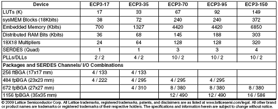

圖1。LatticeECP3-35簡化方框圖(頂層)
LatticeECP3視頻協議板
LatticeECP3 Video Protocol Board
The LatticeECP3™ FPGA family includes many features for video applications. For example, DisplayPort, SMPTE standards (SD-SDI, HD-SDI and 3G-SDI), DVB-ASI, DVI and HDMI can be implemented with 16 channels of embedded SERDES/PCS. 7:1 LVDS video interfaces like ChannelLink and CameraLink can be supported by the generic DDRX2 mode on the I/O pins. When configuring to TRLVDS mode, the I/O pins on banks 0 and 1 can also be used to receive the TMDS signals of DVI or HDMI video standard.
This user’s guide describes revision C of the LatticeECP3 Video Protocol Board featuring the LatticeECP3 LFE3-95E-7FN1156C FPGA device. The stand-alone evaluation PCB provides a functional platform for development and rapid prototyping of many different video applications.
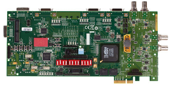
圖2。LatticeECP3視頻協議板外形圖-Rev.C
主要特性:
• Video interfaces for interconnection to video standard equipment
• Allow the demonstration of SD/HD/3G-SDI, DisplayPort and PCI Express (x4) interfaces using SERDES channels
• High speed Mezzanine connector connected to SERDES channels for future expansion
• Allows the demonstration of LVDS video standards – ChannelLink and CameraLink
• Allows control of SERDES PCS registers using the Serial Client Interface (ORCAstra)
• Allows the demonstration of receiving TMDS signals using the DVI interface
• On-board Boot Flash with Serial SPI Flash memory device
• Shows interoperation with high performance DDR2 memory components
• Driver-based “run-time” device configuration capability via an ORCAstra or RS232 interface
• SMAs for external high-speed clock / PLL inputs
• Switches, LEDs and LCD display header for demo purposes
• Mictor connector for using Logic Analyzer in the debugging phase
• Input connection for lab-power supply
• Power connections and power sources
• ispVM™ programming support
• On-board and external reference clock sources
• Various high-speed layout structures
• User-defined input and output points
• Performance monitoring via test headers, LEDs and switches
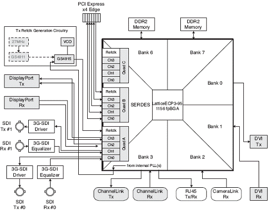
圖3。LatticeECP3視頻協議板-Rev. C功能框圖
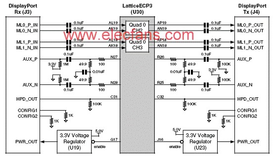
圖4。DisplayPort 視頻接口方框圖

圖5。LatticeECP3視頻協議板方框圖
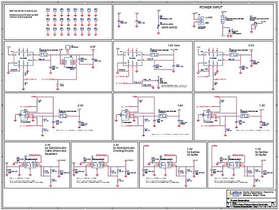
圖6。LatticeECP3視頻協議板電路圖-電源

圖7。LatticeECP3視頻協議板電路圖-電源管理

圖8。LatticeECP3視頻協議板電路圖-FPGA電源
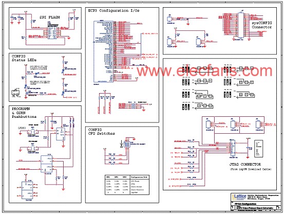
圖9。LatticeECP3視頻協議板電路圖-FPGA配置
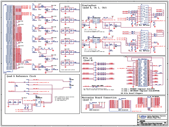
圖10。LatticeECP3視頻協議板電路圖-SERDES
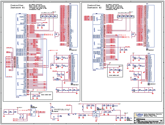
圖11。LatticeECP3視頻協議板電路圖-DDR2存儲器
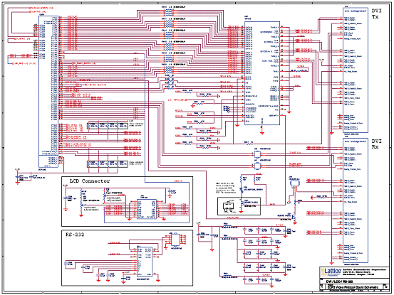
圖12。LatticeECP3視頻協議板電路圖-DVVLCD/RS232

圖13。LatticeECP3視頻協議板電路圖-通路/照相機連接

圖14。LatticeECP3視頻協議板電路圖-TI ADC/CLOCK
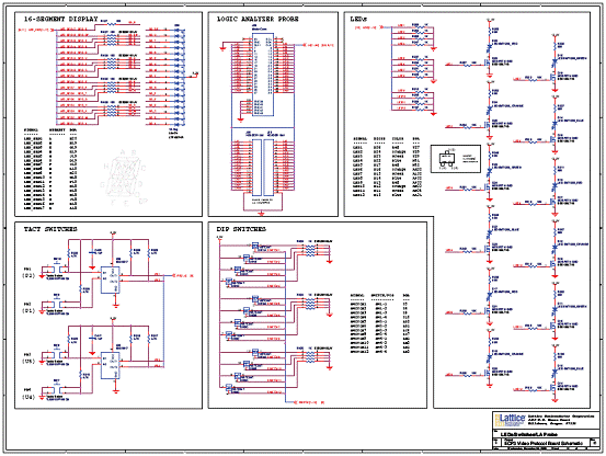
圖15。LatticeECP3視頻協議板電路圖-LED/開關
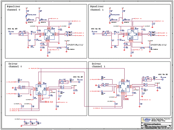
圖16。LatticeECP3視頻協議板電路圖-SDI驅動/均衡器

圖17。LatticeECP3視頻協議板電路圖-SDI基準時鐘控制
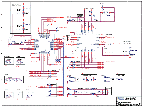
圖18。LatticeECP3視頻協議板電路圖-SRI Rx基準時鐘

圖19。LatticeECP3視頻協議板電路圖-SRI Tx基準時鐘