

ADL5354是高度線性雙平衡(RF和LO平衡)RF混頻器,輸入頻率從2300 MHz 到2900MHz.平衡的無源混頻器具有良好的LO-RF泄漏,優于-35dBm.IF頻率范圍從30MHz到450MHz,功率轉換增益8dB,單邊帶(SSB)噪音10dB,輸入IP3為25dBm,輸入P1為11dBm,LO典型驅動為0dBm.工作電壓3.3V-5.0V,主要用在蜂窩無線基站接收器,無線鏈接下變換器等.本文介紹ADL5354主要特性,方框圖以及典型應用,評估板電路圖和元件配置表.
The ADL5354 uses a highly linear, doubly balanced, passive
mixer core along with integrated RF and local oscillator (LO)
balancing circuitry to allow single-ended operation. The
ADL5354 incorporates the RF baluns, allowing for optimal
performance over a 2300 MHz to 2900 MHz RF input frequency
range. The balanced passive mixer arrangement provides good
LO-to-RF leakage, typically better than −35 dBm, and excellent
intermodulation performance. The balanced mixer core also
provides extremely high input linearity, allowing the device
to be used in demanding cellular applications where in-band
blocking signals may otherwise result in the degradation of
dynamic performance. A high linearity IF buffer amplifier
follows the passive mixer core to yield a typical power
conversion gain of 8.2 dB and can be used with a wide range of
output impedances.
The ADL5354 provides two switched LO paths that can be used in
TDD applications where it is desirable to ping-pong between
two local oscillators. LO current can be externally set using
a resistor to minimize dc current commensurate with the
desired level of performance. For low voltage applications,
the ADL5354 is capable of operation at voltages down to 3.3 V
with substantially reduced current. Under low voltage
operation, an additional logic pin is provided to power down
(<300 μA) the circuit when desired.
The ADL5354 is fabricated using a BiCMOS high performance IC
process. The device is available in a 6 mm × 6 mm, 36-lead
LFCSP and operates over a −40℃ to +85℃ temperature range.
ADL5354主要特性:
RF frequency range of 2300 MHz to 2900 MHz
IF frequency range of 30 MHz to 450 MHz
Power conversion gain: 8 dB
SSB noise figure of 10 dB
Input IP3 of 25 dBm
Input P1dB of 11 dBm
Typical LO drive of 0 dBm
Single-ended, 50 Ω RF and LO input ports
High isolation SPDT LO input switch
Single-supply operation: 3.3 V to 5 V
Exposed paddle, 6 mm × 6 mm, 36-lead LFCSP
ADL5354應用:
Cellular base station receivers
Transmit observation receivers
Radio link downconverters
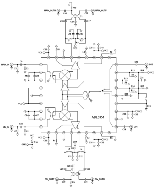
圖1.ADL5354功能方框圖
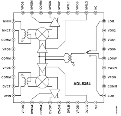
圖2.ADL5354典型應用電路圖
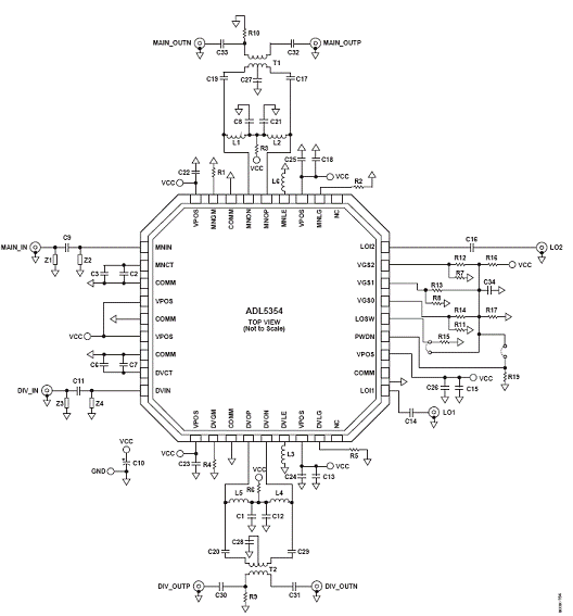
圖3.ADL5354評估板電路圖
ADL5354評估板元件配置表:
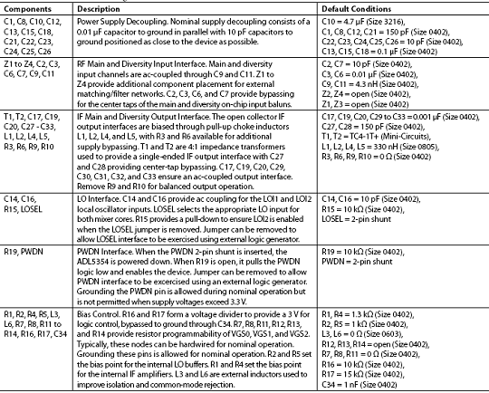
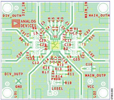
圖4.ADL5354評估板頂層布局圖